SANTA CLARA, Calif.--If you're concerned about the semiconductor memory wall and its impact on electronic system design, don't be.
The semiconductor memory wall is about to be knocked down, and now the challenge is the "CPU wall," according to Mike Black, Technology Strategist, Hybrid Memory Cube Technology, with Micron. Black keynoted the 2013 MemCon here (Aug. 6, 2013), where he described advances in the hybrid memory cube architecture that are going a long way toward knocking the wall over.
Scaling the Semiconductor Memory Wall
Black half-jokingly said:
"This memory wall...we've pushed through. We're teasing some of our CPU partners: ‘Now there's a CPU wall. You guys need to go figure out how to solve that.' We've fixed our end of it and pushed it back into their space."

To recap: The semiconductor memory wall was popularized 20 years ago in a paper by University of Virginia computer scientists William Wulf and Sally McKee. They argued that while both microprocessor and DRAM speed was improving exponentially, CPU speed would outpace DRAM speed eventually:
"The difference between diverging exponentials also grows exponentially; so, although the disparity between processor and memory speed is already an issue, downstream someplace it will be a much bigger one."
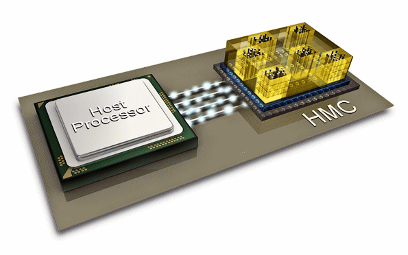
Black told the MemCon audience that the hybrid memory cube approach--stacked DRAMs connected with through-silicon vias (TSV) to a logic layer below--fixes that problem to a degree. It helps electronics designers optimize routing, cuts power consumption significantly and shrinks memory footprint by going vertical (more details below). (Black's colleague, Scott Graham, general manager of Hybrid Memory Cube technology at Micron, offered other insights about HMC technology in a MemCon 2012 keynote).
Memory Bottleneck
Black said microprocessor designers were challenged to optimize the CPU performance and had to wrangle with the memory bottleneck. "They couldn't get enough memory accesses. They couldn't put enough SRAM bits on the CPU to really optimize cores running at performance. So this memory wall was our focus," Black said.
The industry still needs to work diligently on new memory cells but the hybrid memory cube architecture is part of the solution, Black added.
He also noted that while products based on the first-generation HMC spec are expected in the coming quarters, the 110-member Hybrid Memory Cube Consortium's working group is already specifying the second generation, which will double the throughput of Gen 1 approaches, Black said.
Gen 2: Faster
Two interfaces support different PC board trace lengths and signalling rates. The short-reach interface supports 8-10-inch traces, at up to 15Gb/s; the ultra-short reach spec supports 2-3-inch traces, at up to 10Gb/s. The second generation spec will push the short-reach interface to 30 Gb/s and the ultra-short reach to 15 Gb/s or higher. A draft is expected in the next two months, with the full specification due out next year, Black added.
The memory cube consortium claims various benefits over traditional DRAM approaches, including:
- More than 15X the bandwidth of a DDR3 module.
- Greater power efficiency and energy savings, utilizing 70% less energy per bit than DDR3 DRAM technologies.
- Smaller Physical Footprint - The stacked architecture uses nearly 90% less physical space than today's RDIMMs.
The first devices based on the first-generation specifications are due soon. A four-layer 2GB cube will sample in the fourth quarter, while an 8-layer version will sample in the second quarter of next year. Production is expected in the summer of 2014, Black said.
Brian Fuller
Related stories:
--MemCon Keynote: Why Hybrid Memory Cube Will "Revolutionize" System Memory--Semiconductor Memory Challenges Will Be Overcome, MemCon Keynoter Says
--MemCon Samsung Keynote: New DRAM and Flash Memory Architectures are Needed
--MemCon Panel: Promises and Pitfalls of 3D-IC Memory Standards